Preface: This was originally drafted in September 2020, and is only being published ~2 years later. I can’t remember my exact mood when I drafted this article, but apparently it was one of those days. It was also not the first time I’d experienced this issue. I hope posting it here will allow me to not experience this issue again, and help someone else who befalls a similar misfortune.
I hate everything. That’s right. Everything! ARGH! Cue continuos shouts into the void.
Issue: Laptop won’t output audio over HDMI. There is no setting anywhere that seems to allow you to output to HDMI, even though you could swear you’ve done it before. Also every ‘solution’ on the internet tells you to do something you’ve already done or change a setting that doesn’t exist.
Device: Asus FX502VM, Windows 10, GeForce GTX 1060
Early in the pandemic my employer had us working from home. For the most part this was not an issue. But not having a dedicated office, I found it too easy to lose track of time, and spend too much (in my opinion) time working. With my computer set up in our lounge, it was too easy to check an email, or quickly test something else. It was right there.
There was also no separation that came from cycling/taking the train to or from work. Wake up in the morning, sit down at the desk with breakfast/coffee, start working. Without planned events in the evening, continuing to work was easy.
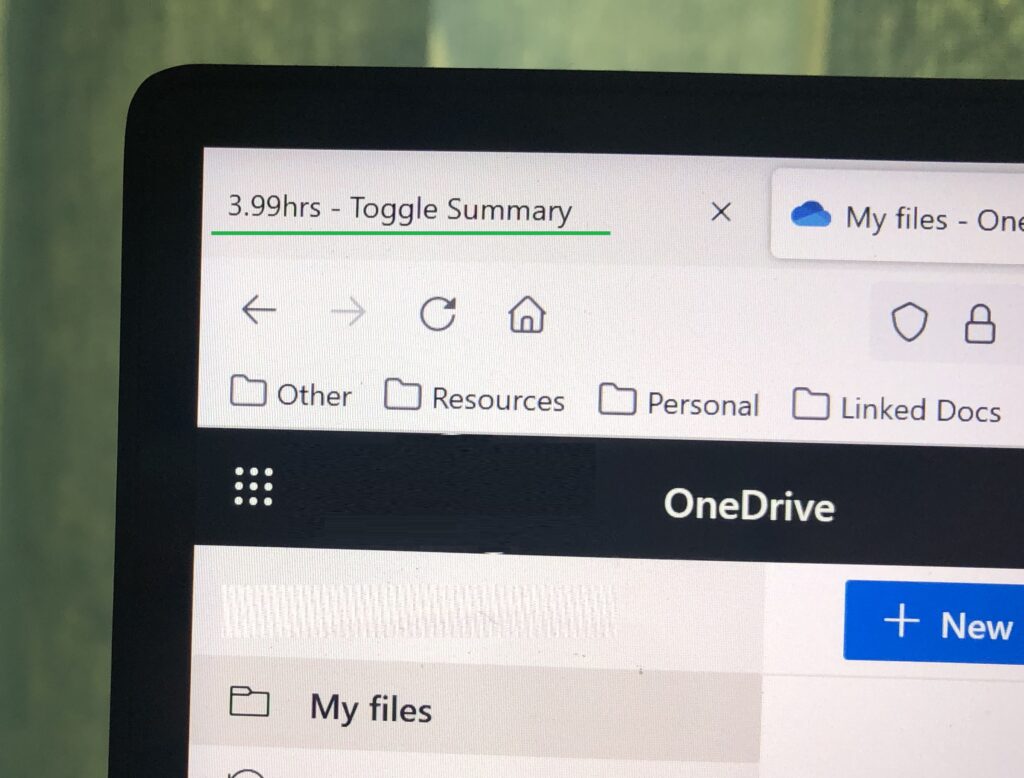
In an effort to limit this I once again repurposed my Particle Internet Button to do some time tracking. I’d used Toggl in the past to do some time tracking, but liked the idea of having a visual display available to me, without having to pull out my phone, or install additional applications on my work laptop.
My basic idea was to use the Particle Internet Button as a switch and display mechanism for interfacing with the Toggl API. The main issue I encountered with this approach was that Toggl was enforcing https for their API calls (and rightly so), but there were complications around the available Particle https libraries at the time.
Not wanting to spend the time on figuring that out, I somehow convinced myself that I should just spin up my own “Toggl-like” service. Obviously just for me, and not requiring https :) Hopefully my employer doesn’t hack my Wi-Fi to intercept my network comms and make me think I’m working less than I actually am.
And so that’s what I did. I setup a database, and threw together some php scripts to interpret different requests as start and stop commands, also taking a date-time string as a parameter. I expanded it a bit, allowing for different work-id’s, if I want to track different topics, and protected it all behind a nice long ‘key’ to limit the risk of someone messing with my data.
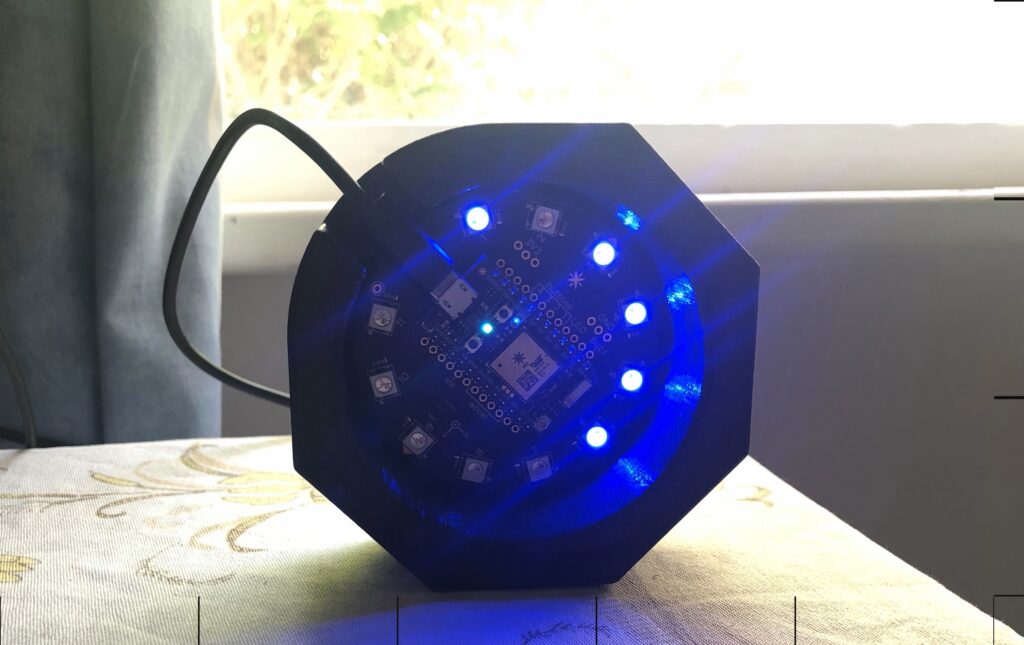
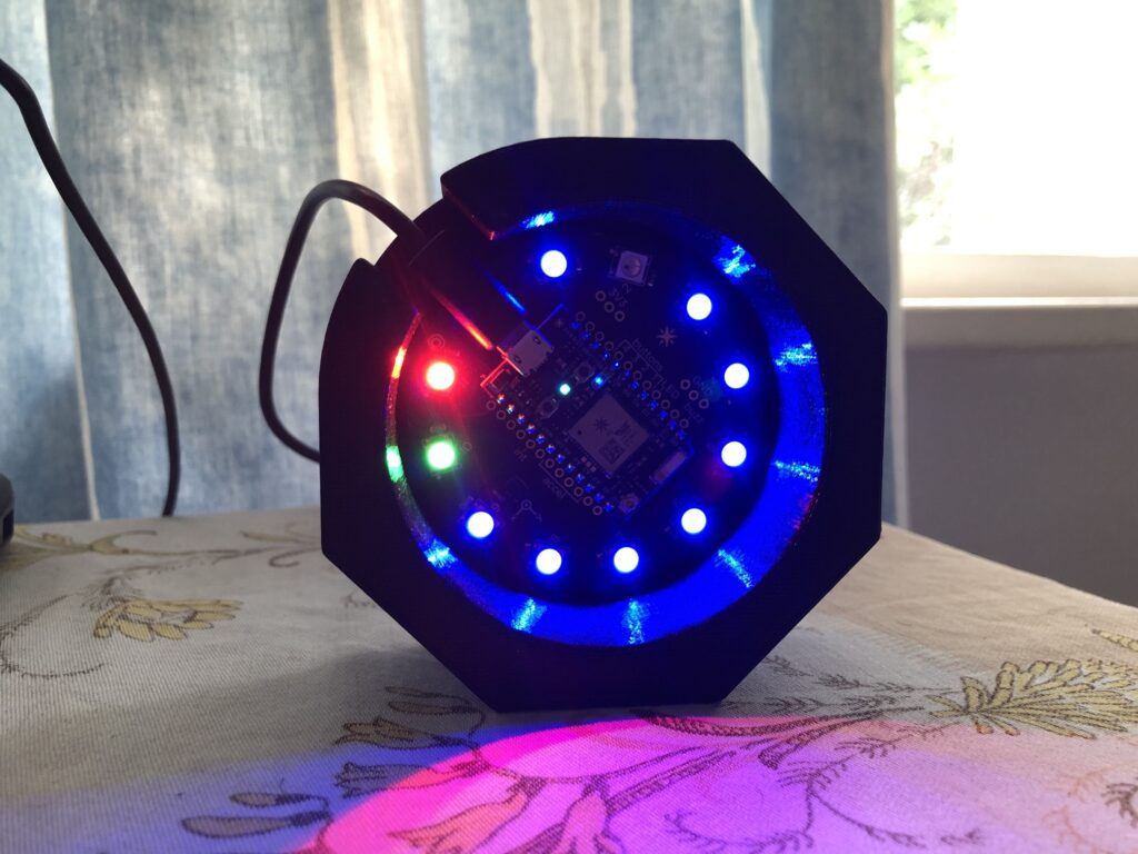
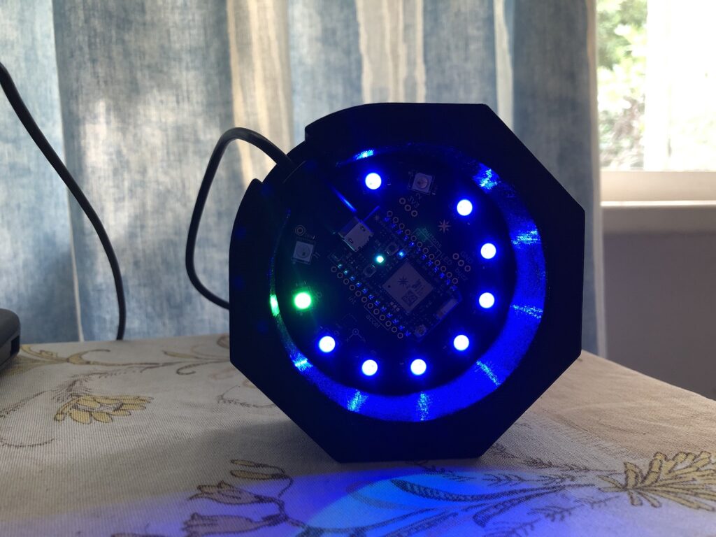
The Internet Button itself is round, and has a bunch of RGB LEDs on it. Eleven LEDs lets me use one for a notification, one as a spacer, and the other nine as hours worked increments. The Internet Button does have buttons that can be used as inputs, but instead I chose to use the accelerometer to give me a more intuitive input, without the need for labels.
I 3D printed an octagon-shaped holder for it, which allows me to rotate the internet button to five fixed locations, which are easily distinguished from each other by the accelerometer. If you’re in the central position, the timer stops. If you shift to one of the other four positions, you start the timer associated with that position. In practice I’m only using one, so the other’s are mostly untested for now.
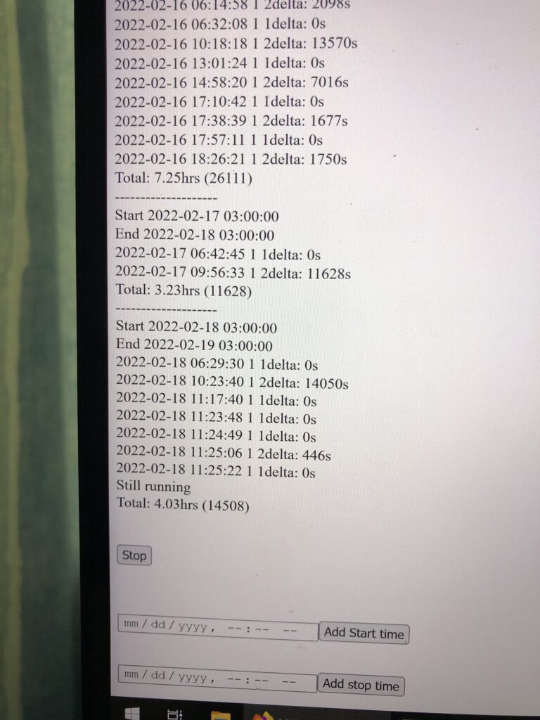
If I don’t have the hardware with me at any time, there’s also a basic web-interface, that allows me to view the entire week’s hours worked, and each stop and start event. I can also add events if I forgot to start or stop at some time.
Here you can find a link to a GitHub repo with some associated code: link
Below you can see a video of it working, and interspersed in this article are a couple photos of different stages.
I bought this watch back in ~2013 and used it track my runs for several years. I recently got an Android watch which also had a built-in GPS, so gave the Nike+ SportWatch to my wife. After a few months of using it, she could no longer download her runs. I wrote about this previously.
With no real use for it, I decided I’d open it up and see what makes it tick.
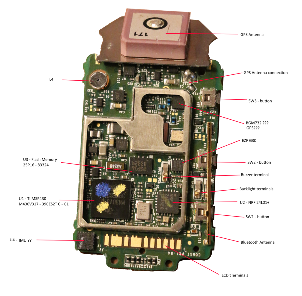
While iFixit has some nice photo guides to disassemble and replace different components, and someone even replaced the entire USB cable, this video shows a complete teardown and takes a look at some of the components used inside the now defunct Nike+ SportWatch.
The teardown is pretty straightforward. There are 6 screws on the back of the watch, that once cleaned of accumulated dirt come off quite easily. The back then separates from the front, with a half of the strap attached to each.
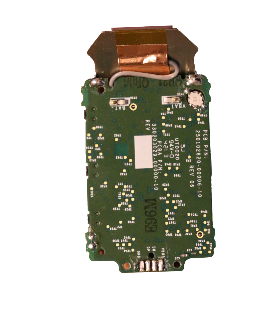
The back half contains the battery, and the front half the rest of the components and USB cable. The USB cable is soldered to the PCBA, so has to be desoldered to continue the teardown. Another two screws hold the PCBA in place.
The LCD comes straight out, but its backlight is held in place by a melted support that must be cut, and has to be unhooked from the bluetooth antenna. The last thing to open up is the shield can, which has many small, tight tabs holding it in place.
Note: this guide specifically shows how I panelized boards to manufacturer with JLCPCB, but the process can probably be applied/modified to fit any PCB fab’s requirements. Also, this is what worked for me in ~March 2020, processes may change, always check for the latest information from your PCB Manufacturer.
A number of PCB manufacturers offer amazing introductory deals for PCB manufacturing. Often this will have a size restriction, in JLCPCB’s case, less than 100x100mm. If you’re making something considerably smaller than this though, you might be able to get multiple boards within that area. But the PCB fabs won’t do the hard work for you, without charging you extra. So why not do it yourself.
For boring rectangular boards, the standard way to do this is using v-grooves cut with a circular saw. Because a circular saw is used, it is only compatible with rectangularly shaped boards. The alternative for irregularly shaped boards is to route the outline of the board, but leave tabs supporting the PCB relative to a frame, or neighbouring PCBs.
One import thing to keep in mind when panelizing boards is how the board will broken apart, especially if your boards are going to be assembled beforehand. It requires putting stress on the boards, which can damage traces and soldered components. For more info on the practicalities of panelizing, read more here.
If you are using Altium Designer to design your board, below are the steps I followed to generate Gerber files that I submitted to JLCPCB. My aim was to get multiple of my boards within the 100x100mm for JLCPCB. I used Altium Designer 19.
In a PCB file, layout your single board including the planned PCB outline.
Create a new PCB file that will contain your panelized design
Set the board shape to be the size of your final panelized design, in my case, 100mmx100mm.
Insert your original PCB design.
Place > Embedded Board Array/Panelize
Push Tab to access the settings
Select your original board under “PCB Document”
Adjust the Column Count, Row Count, and spacing and margin values to get as many of the boards to fit in your limited area. Take into account minimum requirements from your manufacturer, as well as whether you want to have external and/or internal frames around and in between your boards.
If you really want to cram boards in, you can experiment with different rotation of boards so that you don’t waste space. This requires importing the board more than once, with a different rotation specified. Additionally, joining boards to each other, instead of to a frame will also save space. In my case, I didn’t need or want hundreds of copies of this board, I just wanted ten or twenty.
You should now see roughly how your boards will be situated.
To allow for better visualization within Altium’s PCB view, we create a “Route Tool Path” layer to place our routing. User a different Layer Type will allow for correct Gerber generation, but not viewing with Altium’s PCB viewer.
Now we want to create the router patterns to separate our PCBs.
Design > Board Shape > Create Primitives From Board Shape
Select the layer that you want the routing to go on: “Route Tool Path”
For the width of the routing, reference the minimum width requirement specified by the PCB fab.
Select “Route Tool Outline”
You should now have a visible routing path around all your individual PCBs. When you switch to PCB view, you’ll see these as empty spaces.
Notes:
In my example I am separating boards with a frame, if you’re not planning on having a frame, there should be no PCB between each of your boards at this stage.
Because these edges are routed, internal angles can’t be perfectly machined, and will have a radius related to your router width
Now that we have the boards routed, we need to add in breakaway tabs, also known as mouse-bites. This is just a bit of bridging PCB, that has an edge perforated with little holes to make it easier to break off.
To place these in your design, you need to either make a custom part, or create another PCB design that contains just the holes required for your tab. A custom part is better, but both will work.
If you’re linking boards directly to other boards, you want two rows of holes, if you are linking boards to a frame, you only need one row of boards, inline with the edge of the board.
In my example, I have two rows of holes, even though the boards are linked to a frame
The width of the part/board should be the width of your routed edge.
Hole size and spacing should be on your fab’s recommendations.
Based on relative sizes and other factors, you must now decide how many tabs are required to join each of your of your boards, and where they should be located. You must also reference your fab’s recommendations.
For my design I have just two tabs holding each board up.
Once placed, we now have to ‘add’ the material back to support the boards. You can do this by just selecting the relevant part of the route ‘trace’, and either deleting or resizing it.
Switch to PCB view and confirm the resultant tab looks correct.
Now rinse and repeat for all tab locations.
Once you’ve got everything laid out, just make sure to add your entire board outline to your routing layer so they get exported on the same layer. Most fabs expect this. Then all you have to do is export your Gerber files and upload them.
When I actually had the boards manufactured, I only put 5 boards horizontally to a panel of a single row. I also placed the tabs on the sides. As such the below images won’t match what I demonstrated above.
For JLCPCB, this is what my exported board outline layer looked like, as well as how JLCPCB displayed the boards in their Gerber viewer, and how they came out:
At the same time I had the same boards manufactured with OSH Park. They ask for a slightly different layout. They want the outline of the milled area as opposed to a single trace for the mill. As such the board outline layer looked like this (along with how OSH Park displayed it and how they came out).
OSH Park actually offer to do the tabs themselves. You just provide the milling outline around the entire board, and they’ll add the tabs. I don’t recall this being an option when I had the boards made (~March 2020), but it is on their website (Jan 2021).
Below is another design I had manufactured this year for my Touch Lamp. Here I joined boards directly to each other. Below you can see Altium’s PCB view as well as the final product. To achieve this, I had to import my nominal PCB twice, once for the upright orientation, and once for the upside down orientation. In this case, when I exported the Gerber’s, I did not include the rectangle that went around the entire board, as I didn’t want the little triangles included.
If you have any questions, or additional information you think others will find useful, please leave a comment below.