Note: this guide specifically shows how I panelized boards to manufacturer with JLCPCB, but the process can probably be applied/modified to fit any PCB fab’s requirements. Also, this is what worked for me in ~March 2020, processes may change, always check for the latest information from your PCB Manufacturer.
JLCPCB Panelizing notes: link (More under capabilities: link)
OSHPark Panelizing notes: link
A number of PCB manufacturers offer amazing introductory deals for PCB manufacturing. Often this will have a size restriction, in JLCPCB’s case, less than 100x100mm. If you’re making something considerably smaller than this though, you might be able to get multiple boards within that area. But the PCB fabs won’t do the hard work for you, without charging you extra. So why not do it yourself.
For boring rectangular boards, the standard way to do this is using v-grooves cut with a circular saw. Because a circular saw is used, it is only compatible with rectangularly shaped boards. The alternative for irregularly shaped boards is to route the outline of the board, but leave tabs supporting the PCB relative to a frame, or neighbouring PCBs.
One import thing to keep in mind when panelizing boards is how the board will broken apart, especially if your boards are going to be assembled beforehand. It requires putting stress on the boards, which can damage traces and soldered components. For more info on the practicalities of panelizing, read more here.
If you are using Altium Designer to design your board, below are the steps I followed to generate Gerber files that I submitted to JLCPCB. My aim was to get multiple of my boards within the 100x100mm for JLCPCB. I used Altium Designer 19.
- In a PCB file, layout your single board including the planned PCB outline.

- Create a new PCB file that will contain your panelized design
- Set the board shape to be the size of your final panelized design, in my case, 100mmx100mm.
- Insert your original PCB design.
- Place > Embedded Board Array/Panelize
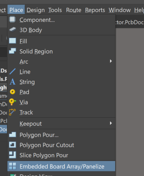
- Push Tab to access the settings
- Select your original board under “PCB Document”
- Adjust the Column Count, Row Count, and spacing and margin values to get as many of the boards to fit in your limited area. Take into account minimum requirements from your manufacturer, as well as whether you want to have external and/or internal frames around and in between your boards.
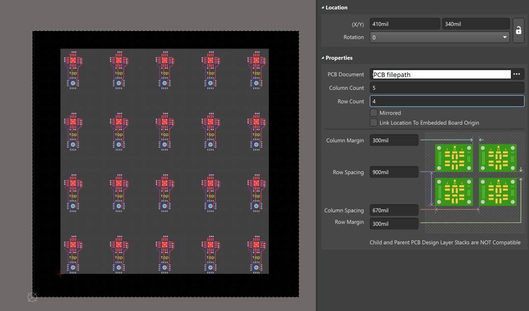
If you really want to cram boards in, you can experiment with different rotation of boards so that you don’t waste space. This requires importing the board more than once, with a different rotation specified. Additionally, joining boards to each other, instead of to a frame will also save space. In my case, I didn’t need or want hundreds of copies of this board, I just wanted ten or twenty.
- You should now see roughly how your boards will be situated.
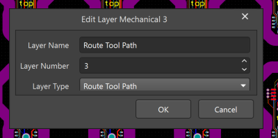
- To allow for better visualization within Altium’s PCB view, we create a “Route Tool Path” layer to place our routing. User a different Layer Type will allow for correct Gerber generation, but not viewing with Altium’s PCB viewer.
- Now we want to create the router patterns to separate our PCBs.
- Design > Board Shape > Create Primitives From Board Shape
- Select the layer that you want the routing to go on: “Route Tool Path”
- For the width of the routing, reference the minimum width requirement specified by the PCB fab.
- Select “Route Tool Outline”
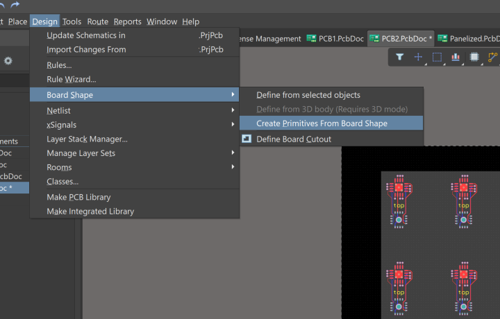
- You should now have a visible routing path around all your individual PCBs. When you switch to PCB view, you’ll see these as empty spaces.
- Notes:
- In my example I am separating boards with a frame, if you’re not planning on having a frame, there should be no PCB between each of your boards at this stage.
- Because these edges are routed, internal angles can’t be perfectly machined, and will have a radius related to your router width

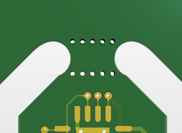
- Now that we have the boards routed, we need to add in breakaway tabs, also known as mouse-bites. This is just a bit of bridging PCB, that has an edge perforated with little holes to make it easier to break off.
- To place these in your design, you need to either make a custom part, or create another PCB design that contains just the holes required for your tab. A custom part is better, but both will work.
- If you’re linking boards directly to other boards, you want two rows of holes, if you are linking boards to a frame, you only need one row of boards, inline with the edge of the board.
- In my example, I have two rows of holes, even though the boards are linked to a frame
- The width of the part/board should be the width of your routed edge.
- Hole size and spacing should be on your fab’s recommendations.
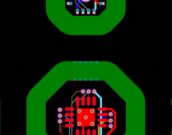
- Based on relative sizes and other factors, you must now decide how many tabs are required to join each of your of your boards, and where they should be located. You must also reference your fab’s recommendations.
- For my design I have just two tabs holding each board up.
- Once placed, we now have to ‘add’ the material back to support the boards. You can do this by just selecting the relevant part of the route ‘trace’, and either deleting or resizing it.
- Switch to PCB view and confirm the resultant tab looks correct.
- Now rinse and repeat for all tab locations.
Once you’ve got everything laid out, just make sure to add your entire board outline to your routing layer so they get exported on the same layer. Most fabs expect this. Then all you have to do is export your Gerber files and upload them.
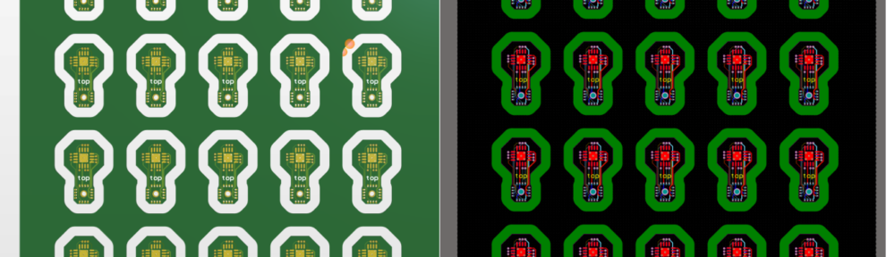
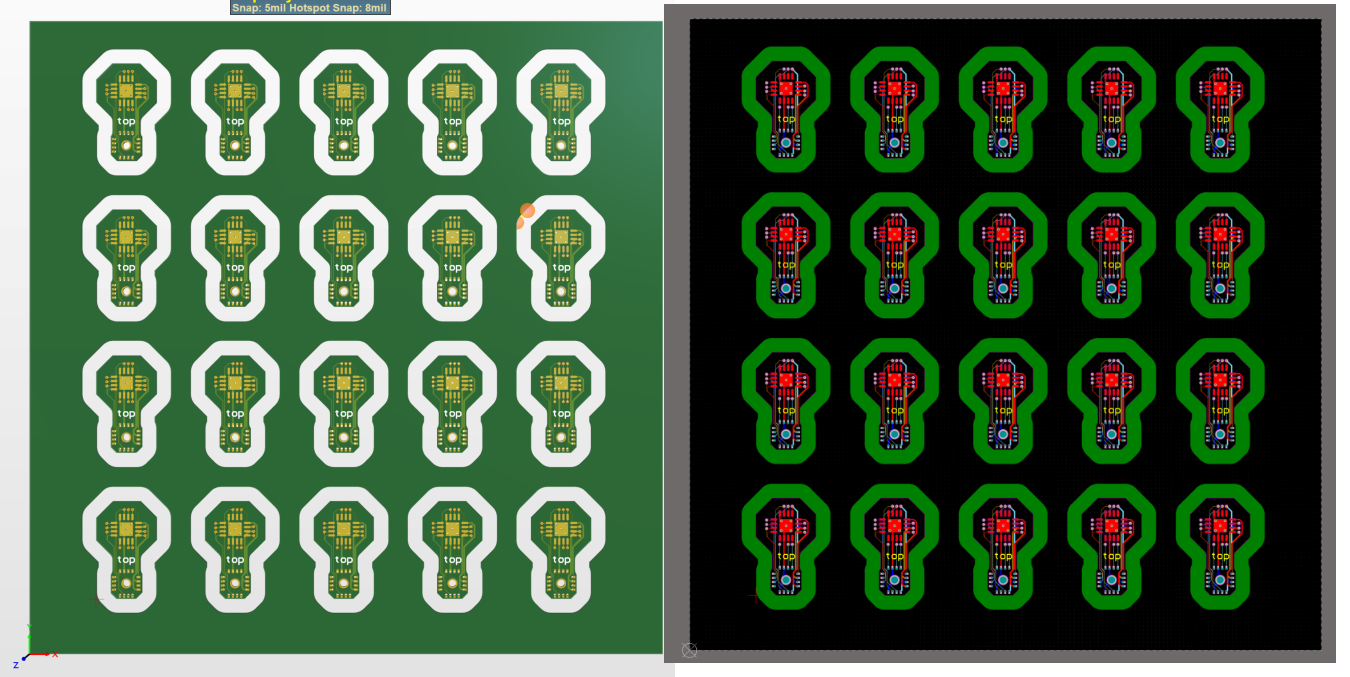
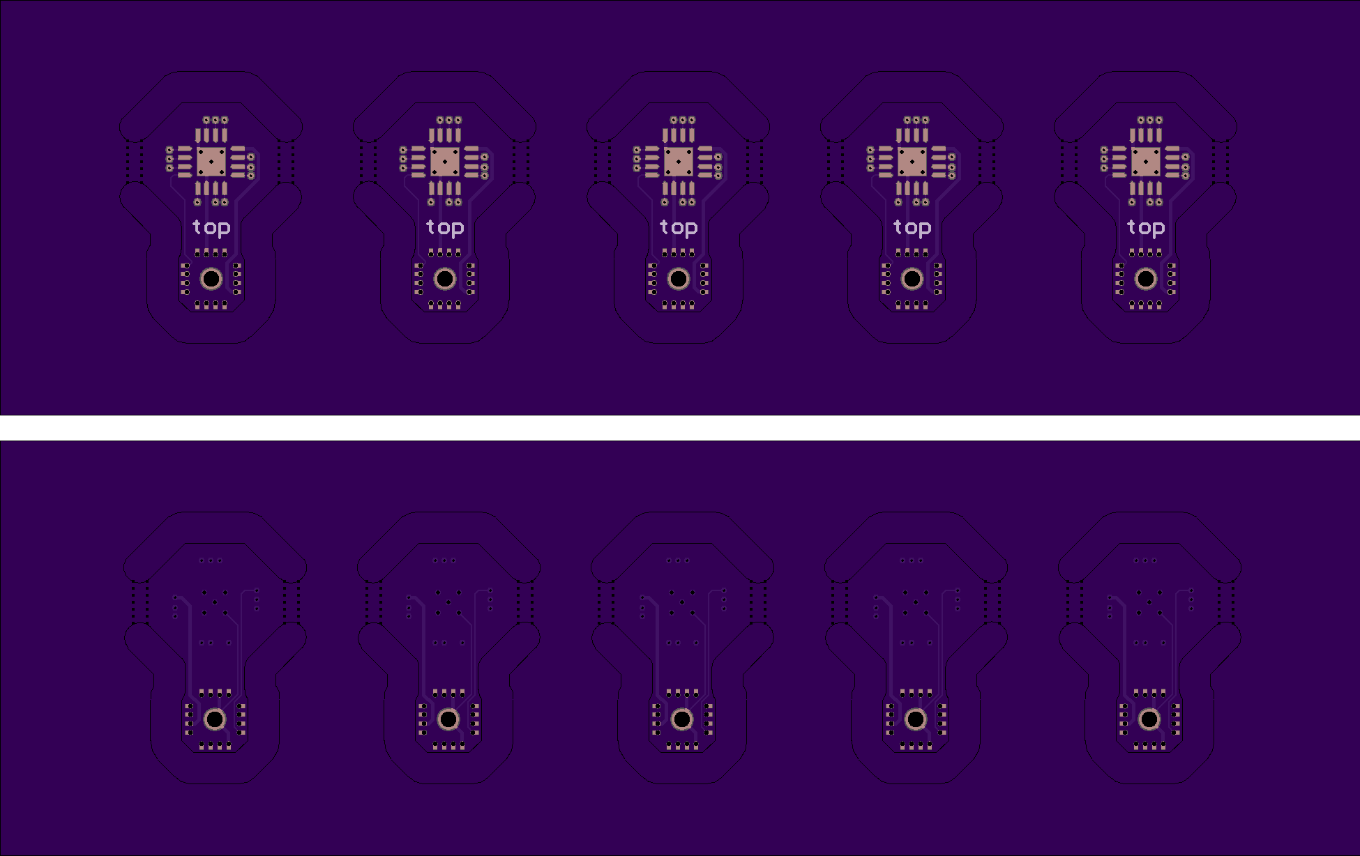
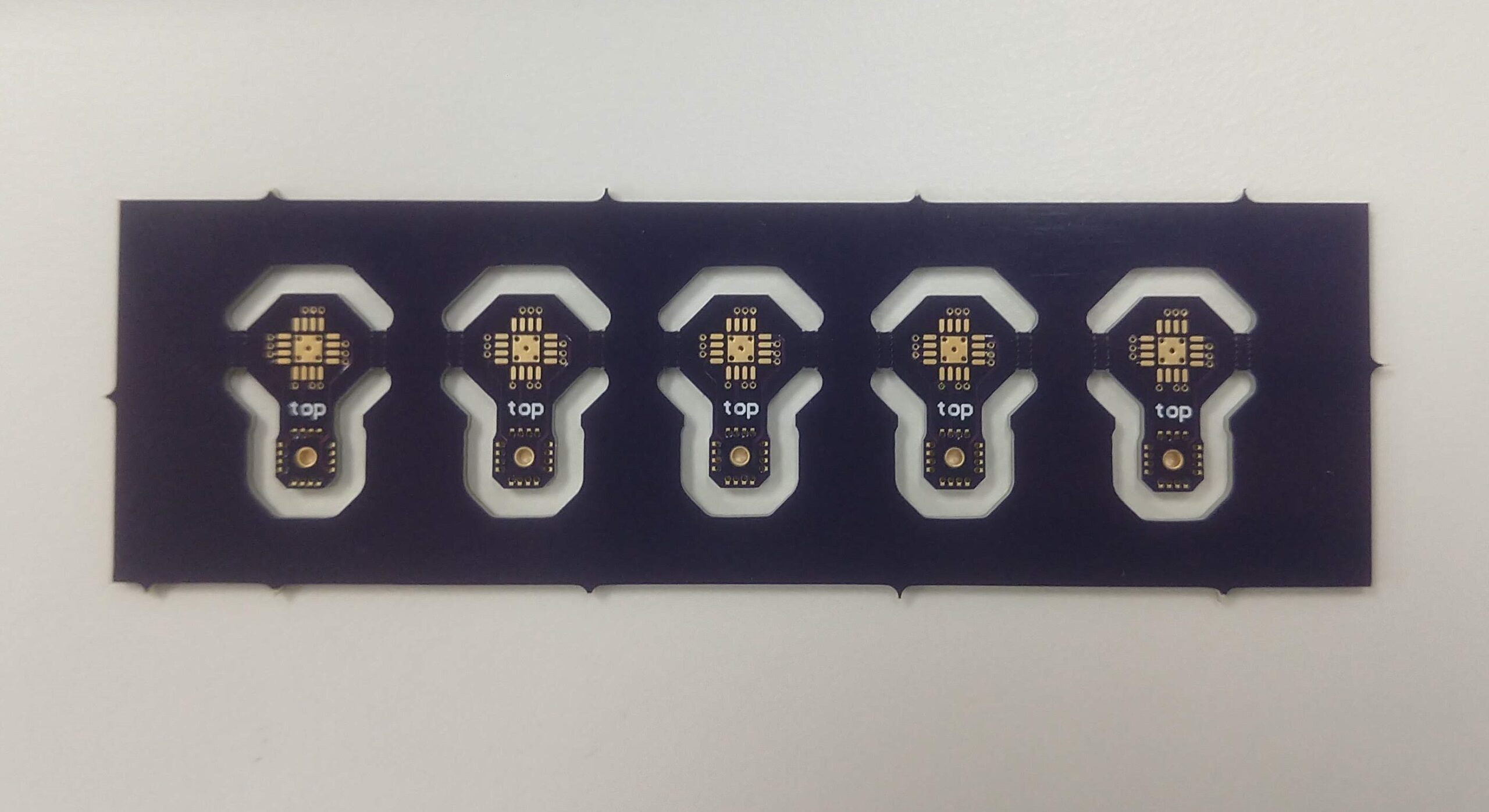
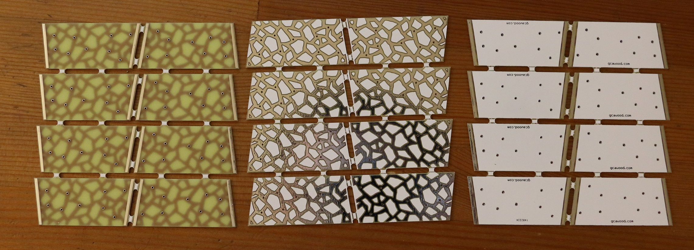
When I actually had the boards manufactured, I only put 5 boards horizontally to a panel of a single row. I also placed the tabs on the sides. As such the below images won’t match what I demonstrated above.
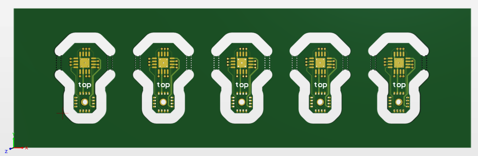
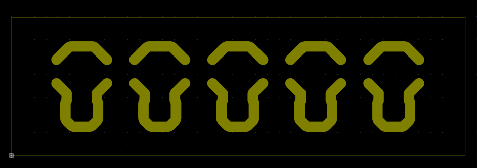
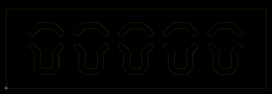
For JLCPCB, this is what my exported board outline layer looked like, as well as how JLCPCB displayed the boards in their Gerber viewer, and how they came out:
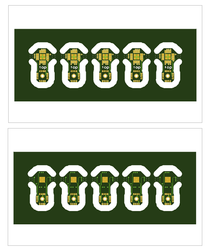

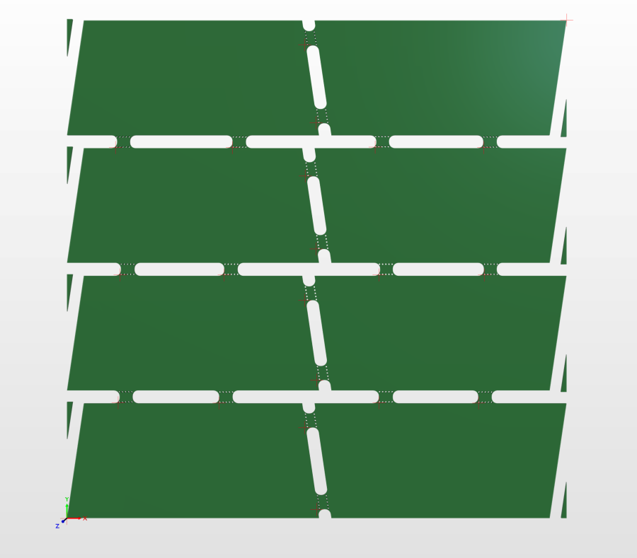
At the same time I had the same boards manufactured with OSH Park. They ask for a slightly different layout. They want the outline of the milled area as opposed to a single trace for the mill. As such the board outline layer looked like this (along with how OSH Park displayed it and how they came out).
OSH Park actually offer to do the tabs themselves. You just provide the milling outline around the entire board, and they’ll add the tabs. I don’t recall this being an option when I had the boards made (~March 2020), but it is on their website (Jan 2021).
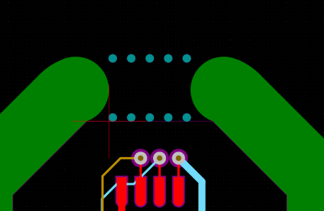
Below is another design I had manufactured this year for my Touch Lamp. Here I joined boards directly to each other. Below you can see Altium’s PCB view as well as the final product. To achieve this, I had to import my nominal PCB twice, once for the upright orientation, and once for the upside down orientation. In this case, when I exported the Gerber’s, I did not include the rectangle that went around the entire board, as I didn’t want the little triangles included.
If you have any questions, or additional information you think others will find useful, please leave a comment below.
Cool design for a lamp shade. Do you have a picture of the final lamp?
Hey Paul, you can see my post here with more on the lamp: https://blog.gcawood.com/2020/10/20/circuit-sculpture-touch-lamp-with-pcb-shade/
hello Gareth, thanks a lot for very detailed write up. I am in the process of learning all that penalization business for very same reason that you mentioned in the beginning of your article and and your explanations are very helpful for me .
there is my question – how whole process would be different if my original PCB has been designed not by Altium and I have full set of Gerbers generated by another SW .
thank you in advance and G-d bless
Hi Michael,
Sorry, I haven’t done that before. I’m sure there are specific tools you could use to duplicate the Gerbers.
Alternatively you may be able to import the Gerbers into Altium, and then attempt the same steps.
Good luck