Early in the pandemic my employer had us working from home. For the most part this was not an issue. But not having a dedicated office, I found it too easy to lose track of time, and spend too much (in my opinion) time working. With my computer set up in our lounge, it was too easy to check an email, or quickly test something else. It was right there.
There was also no separation that came from cycling/taking the train to or from work. Wake up in the morning, sit down at the desk with breakfast/coffee, start working. Without planned events in the evening, continuing to work was easy.
In an effort to limit this I once again repurposed my Particle Internet Button to do some time tracking. I’d used Toggl in the past to do some time tracking, but liked the idea of having a visual display available to me, without having to pull out my phone, or install additional applications on my work laptop.
My basic idea was to use the Particle Internet Button as a switch and display mechanism for interfacing with the Toggl API. The main issue I encountered with this approach was that Toggl was enforcing https for their API calls (and rightly so), but there were complications around the available Particle https libraries at the time.
Not wanting to spend the time on figuring that out, I somehow convinced myself that I should just spin up my own “Toggl-like” service. Obviously just for me, and not requiring https :) Hopefully my employer doesn’t hack my Wi-Fi to intercept my network comms and make me think I’m working less than I actually am.
And so that’s what I did. I setup a database, and threw together some php scripts to interpret different requests as start and stop commands, also taking a date-time string as a parameter. I expanded it a bit, allowing for different work-id’s, if I want to track different topics, and protected it all behind a nice long ‘key’ to limit the risk of someone messing with my data.

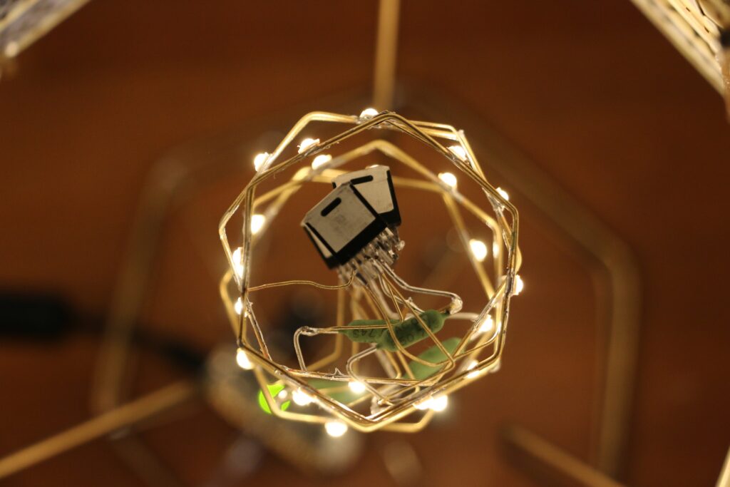
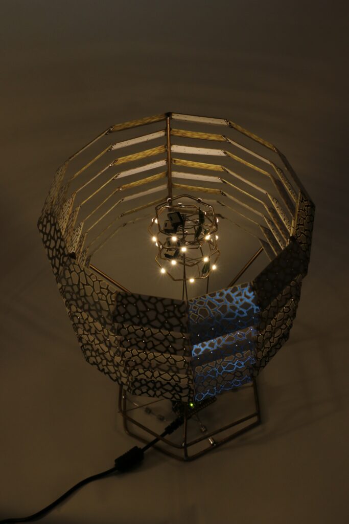
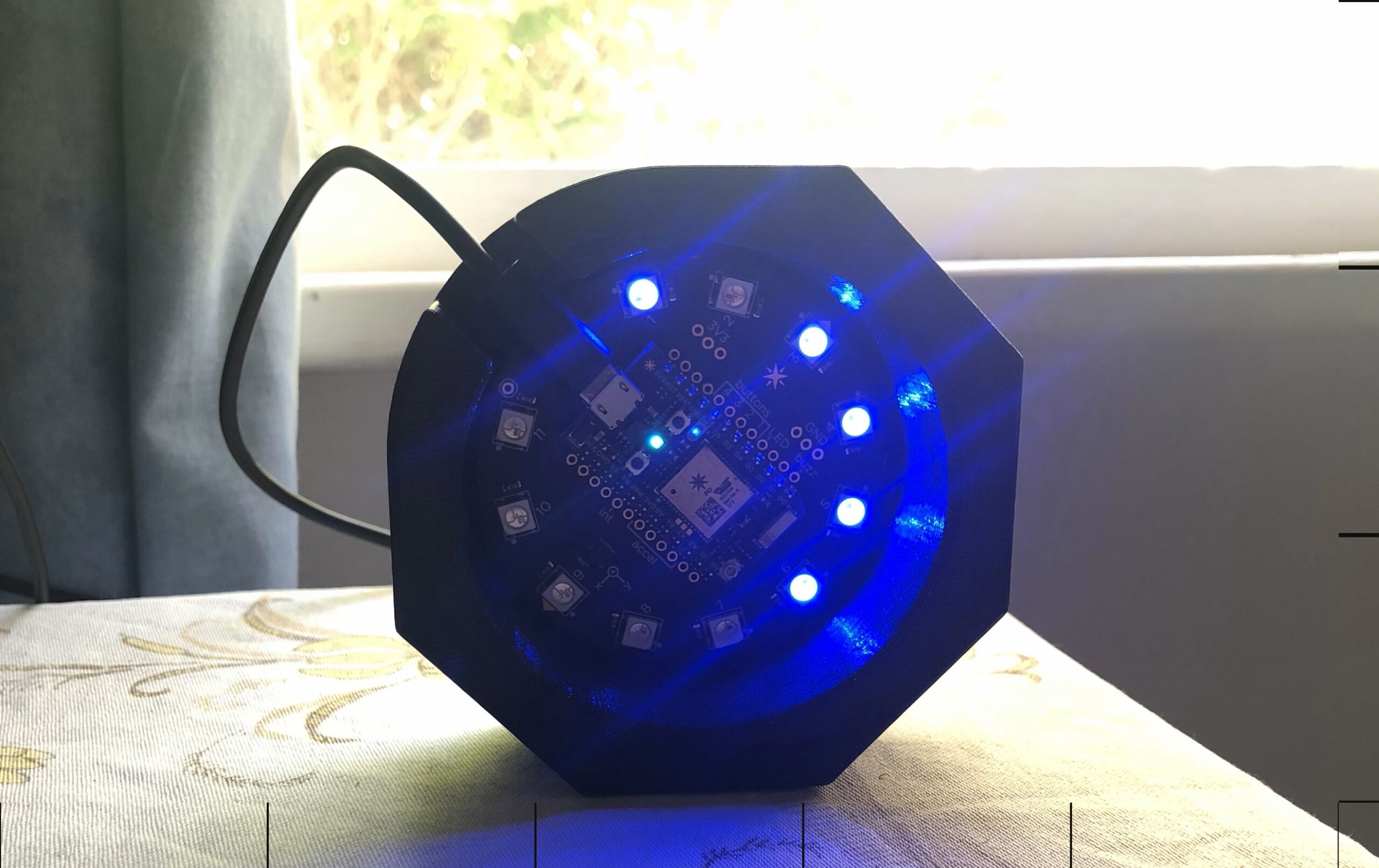
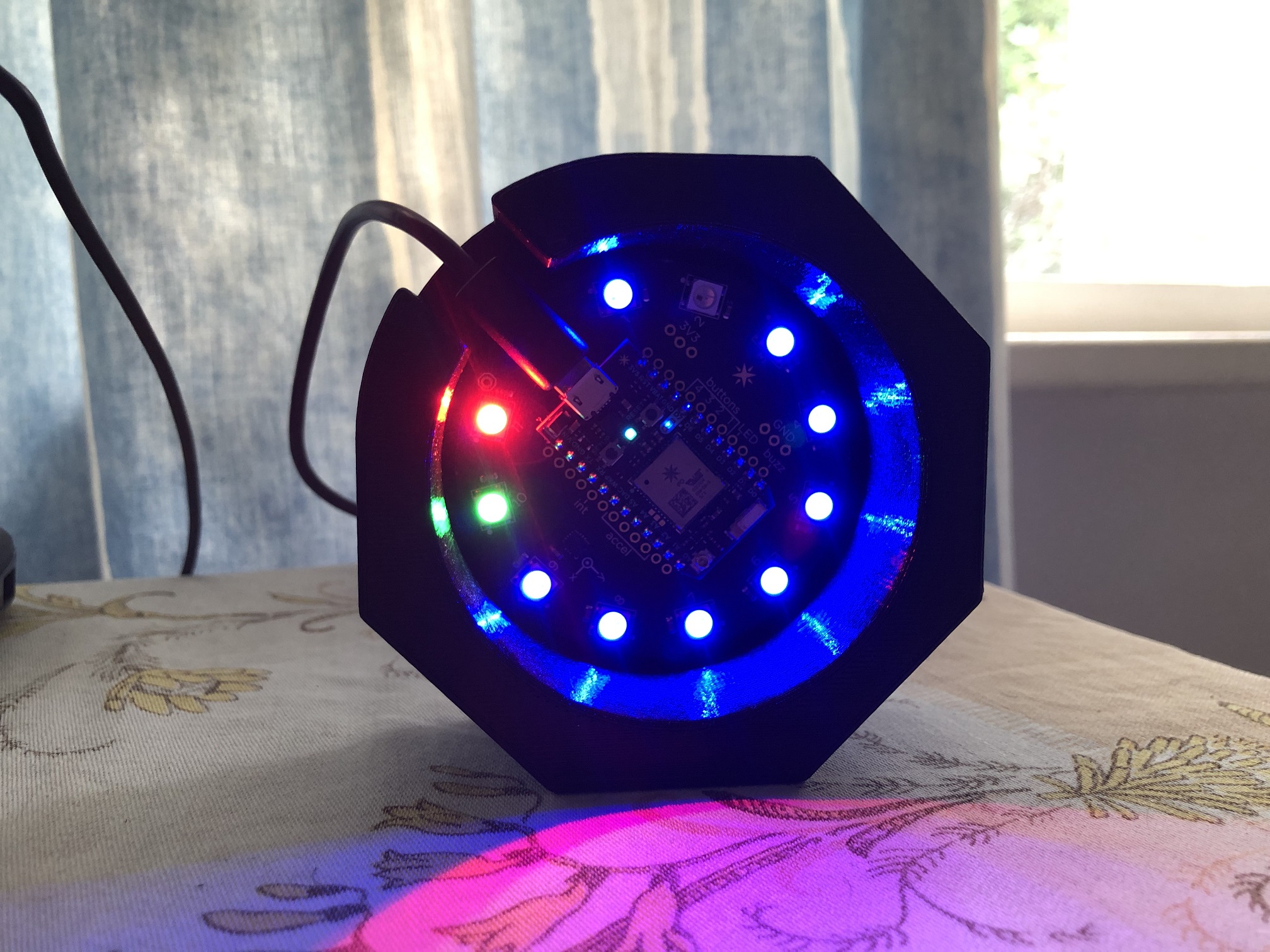
The Internet Button itself is round, and has a bunch of RGB LEDs on it. Eleven LEDs lets me use one for a notification, one as a spacer, and the other nine as hours worked increments. The Internet Button does have buttons that can be used as inputs, but instead I chose to use the accelerometer to give me a more intuitive input, without the need for labels.

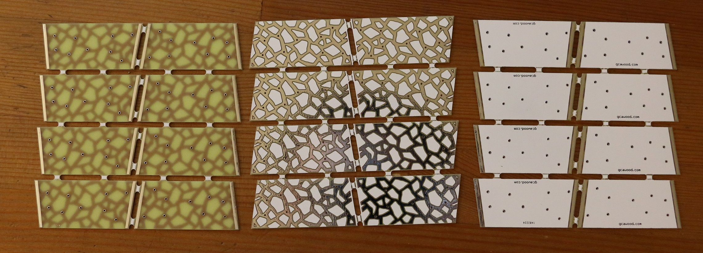
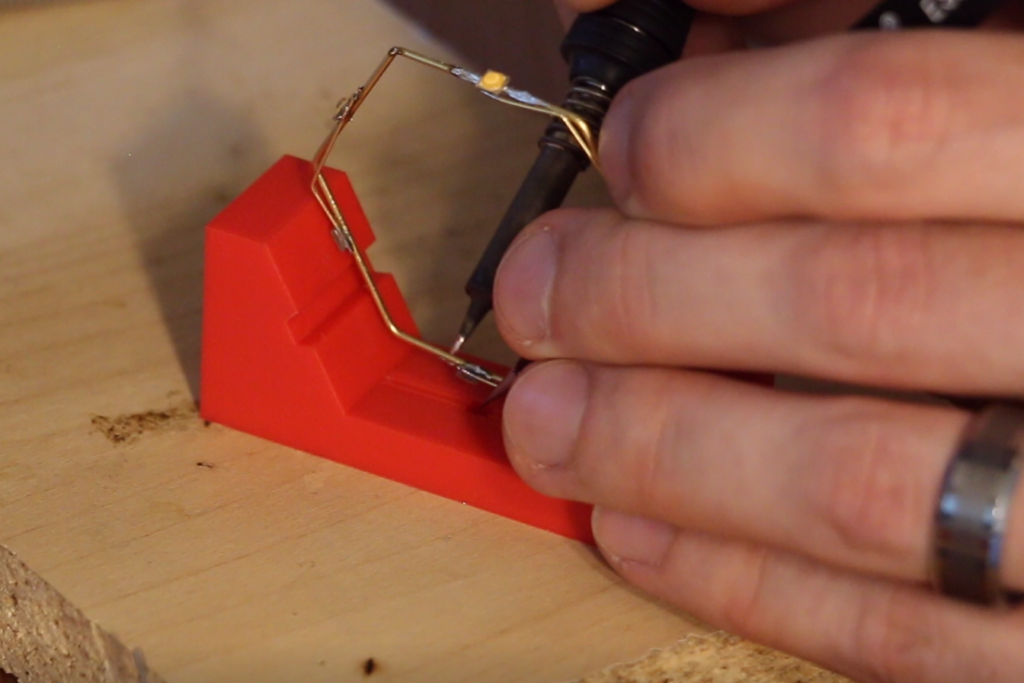
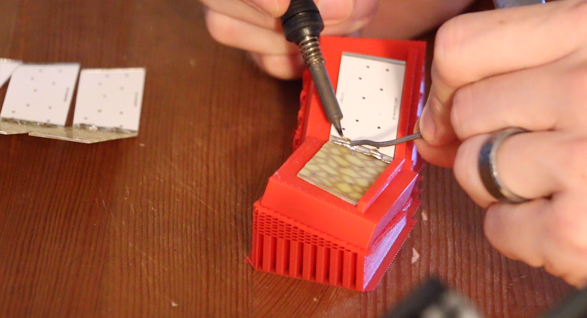
I 3D printed an octagon-shaped holder for it, which allows me to rotate the internet button to five fixed locations, which are easily distinguished from each other by the accelerometer. If you’re in the central position, the timer stops. If you shift to one of the other four positions, you start the timer associated with that position. In practice I’m only using one, so the other’s are mostly untested for now.
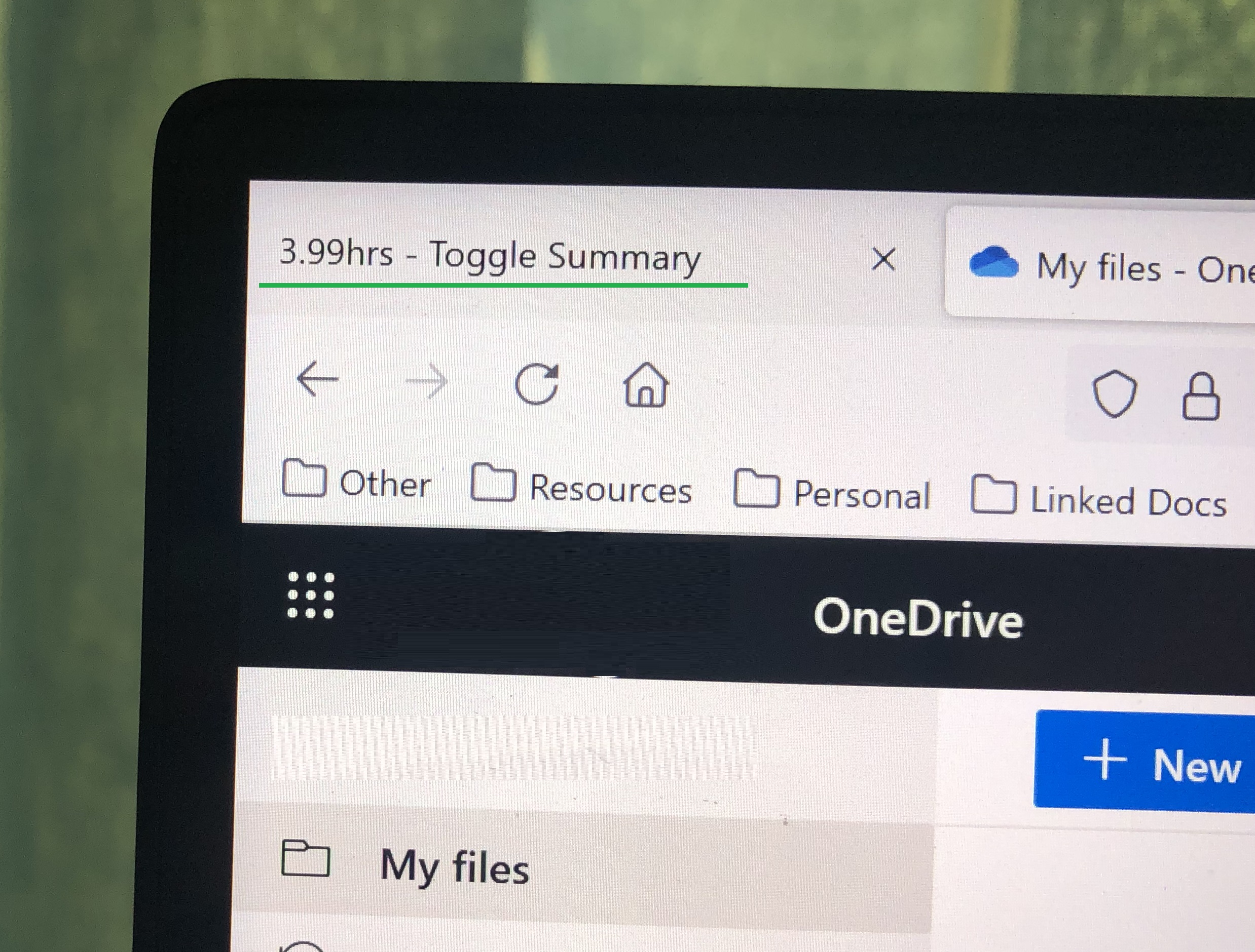
If I don’t have the hardware with me at any time, there’s also a basic web-interface, that allows me to view the entire week’s hours worked, and each stop and start event. I can also add events if I forgot to start or stop at some time.
Here you can find a link to a GitHub repo with some associated code: link
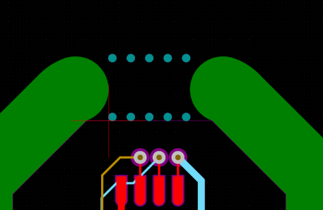
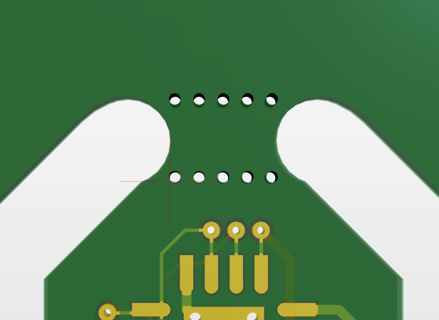
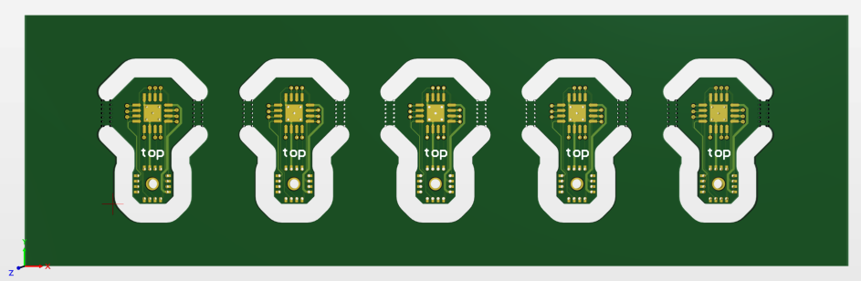
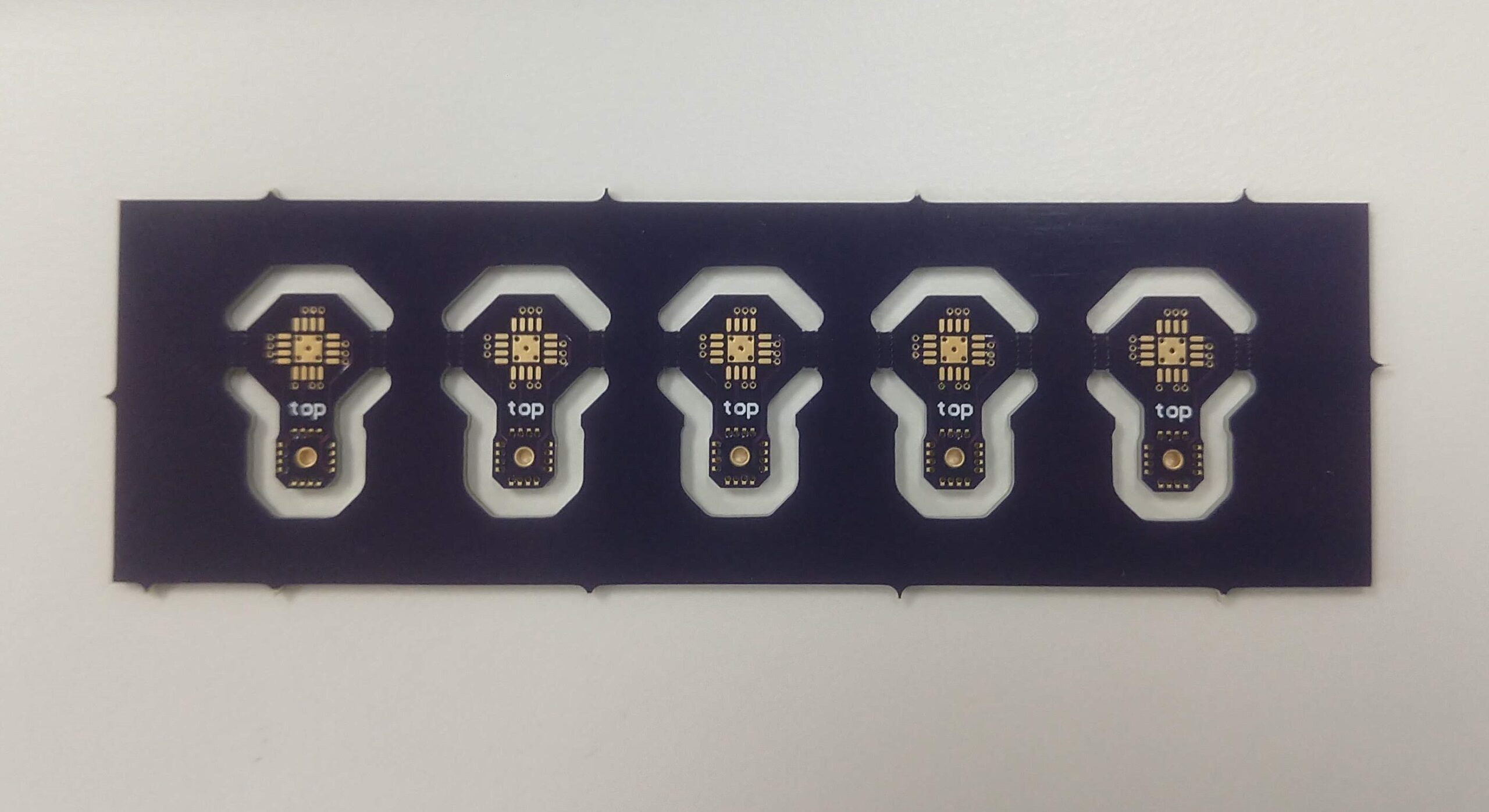
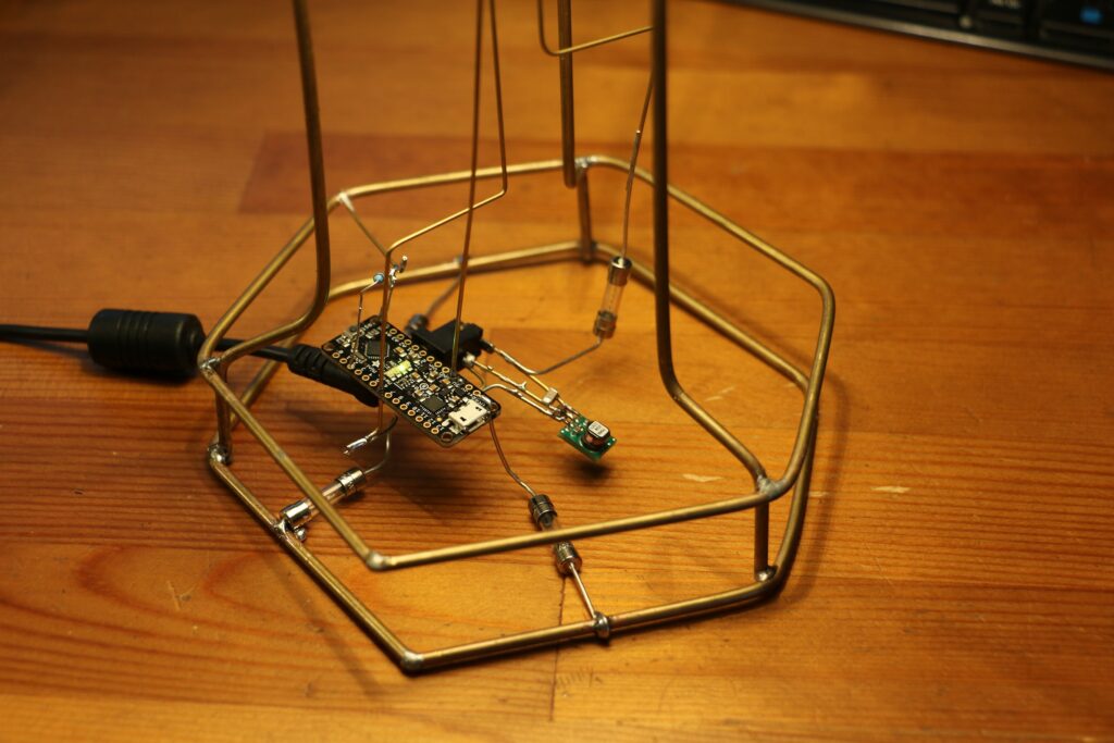
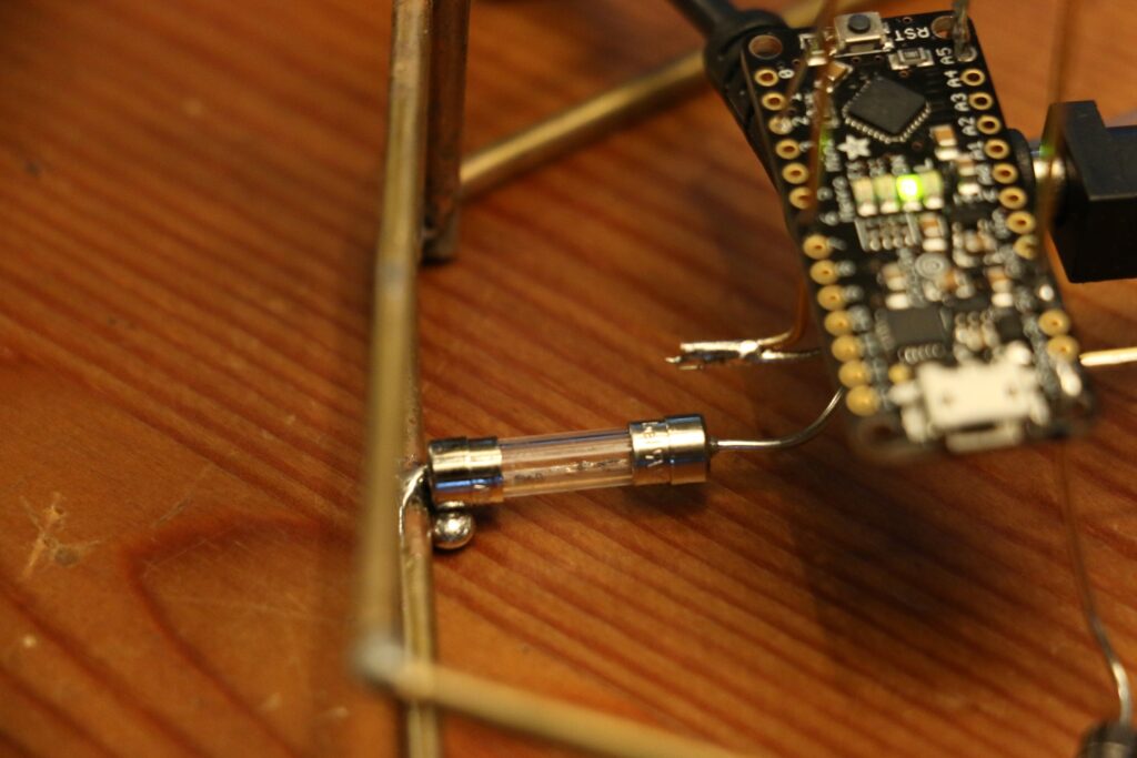
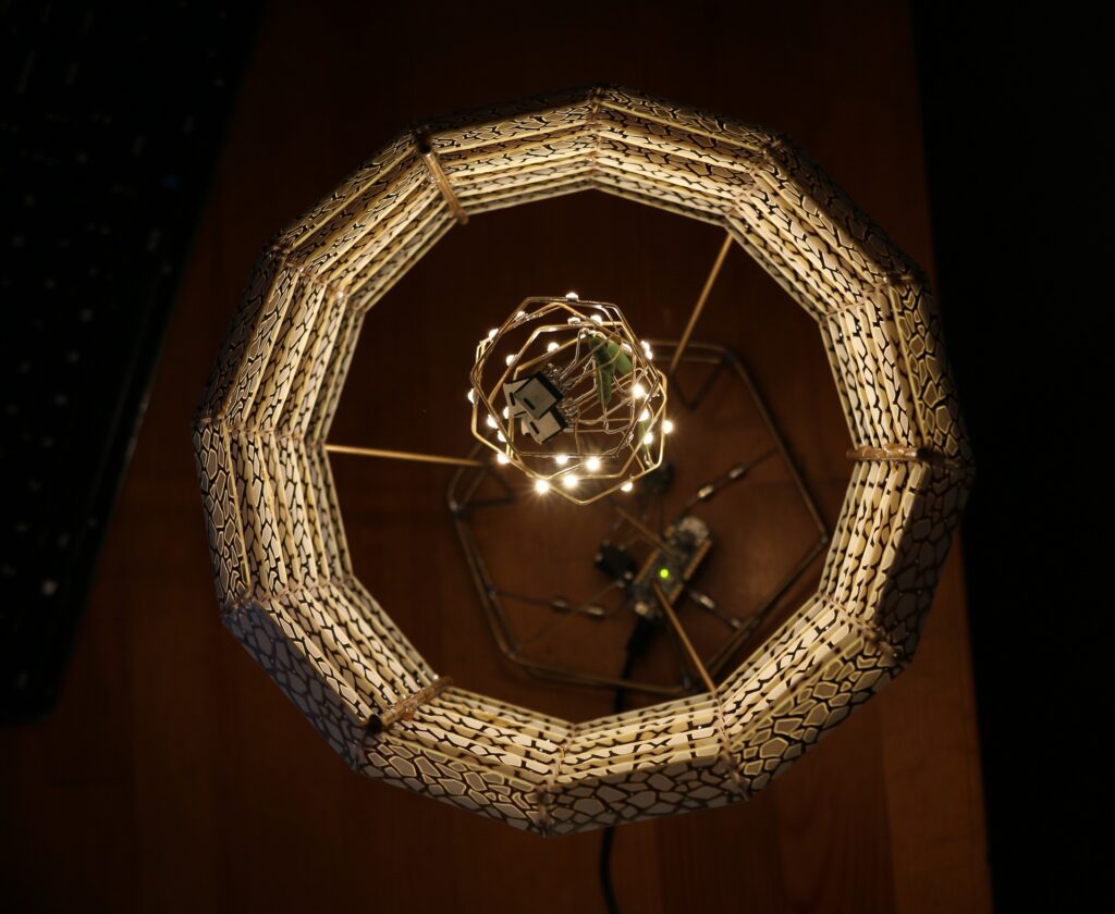
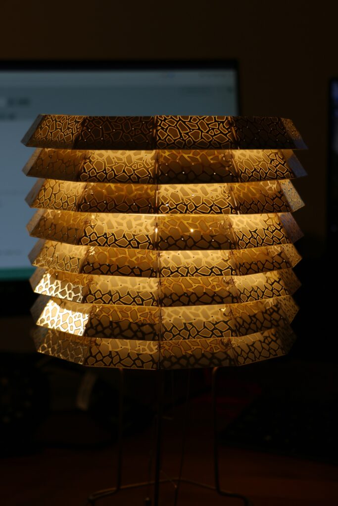
Below you can see a video of it working, and interspersed in this article are a couple photos of different stages.